The project must meet the following requirements:
- 2D/3D designed parts
- CNC machined parts
- Embedded microcontroller that you designed + fabricated
- At least 1 input/output device that interacts with the user
- Embedded programming
Thus, for this project I decided to make a mini game controller.
The PCB can be machined and soldered, the controller case can be machined with a CNC machine.
PCB Design
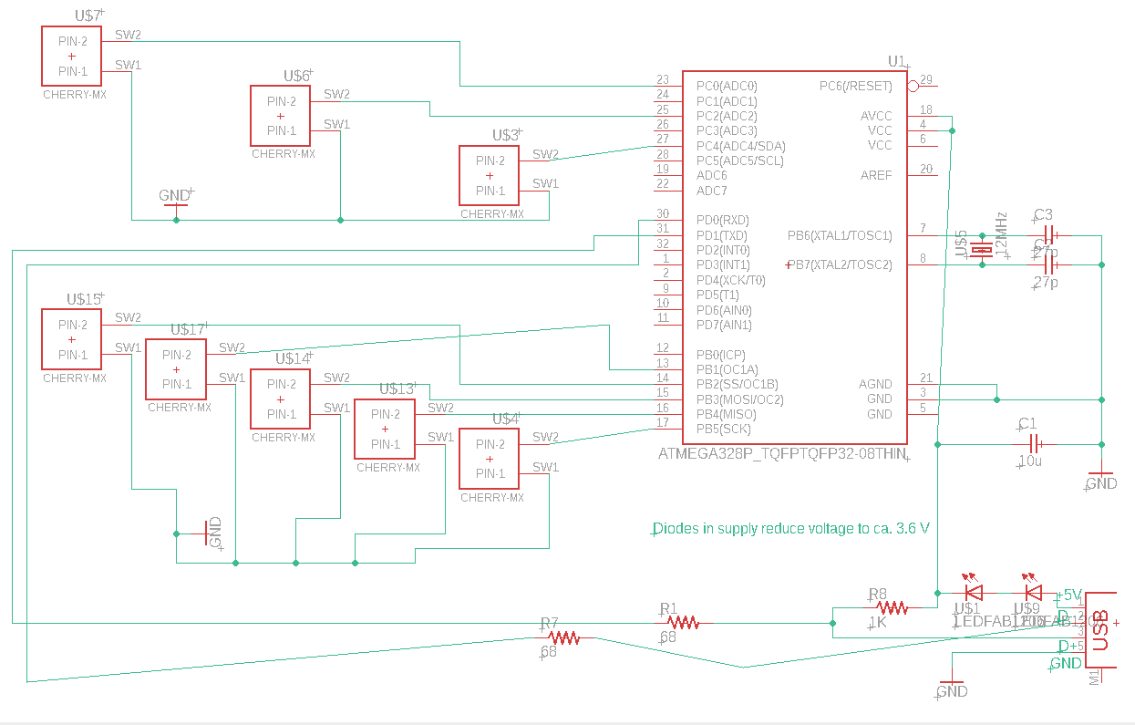
PCB designing was a necessary but painful part of this project. Because of my lack off knowledge of the atmega chip I used, I made lots of changes midway.
For my first attempt, I designed the board to fit everything I needed. This included using FTDI headers to connect my switches, as well as ample space to connect my switches on the board itself.
This idea was later scrapped as having a larger board meant that machining it would be much harder in the sense that there is more room for error.
Larger boards tend to be more unstable with vibrations and holding it down was much harder than usual.
Thus for my second design, I decided to separate the switches from the main PCB. They would still be connected by jumper cables, but the switches will be held on by laser cut plates instead.
With a smaller board and lesser connections to worry about, the board was more compact and easier to mill. This also made the modelling of my controller case easier.
However, as you will see later, I made a few fatal mistakes. First was not accounting for both VCC aand GND connections.
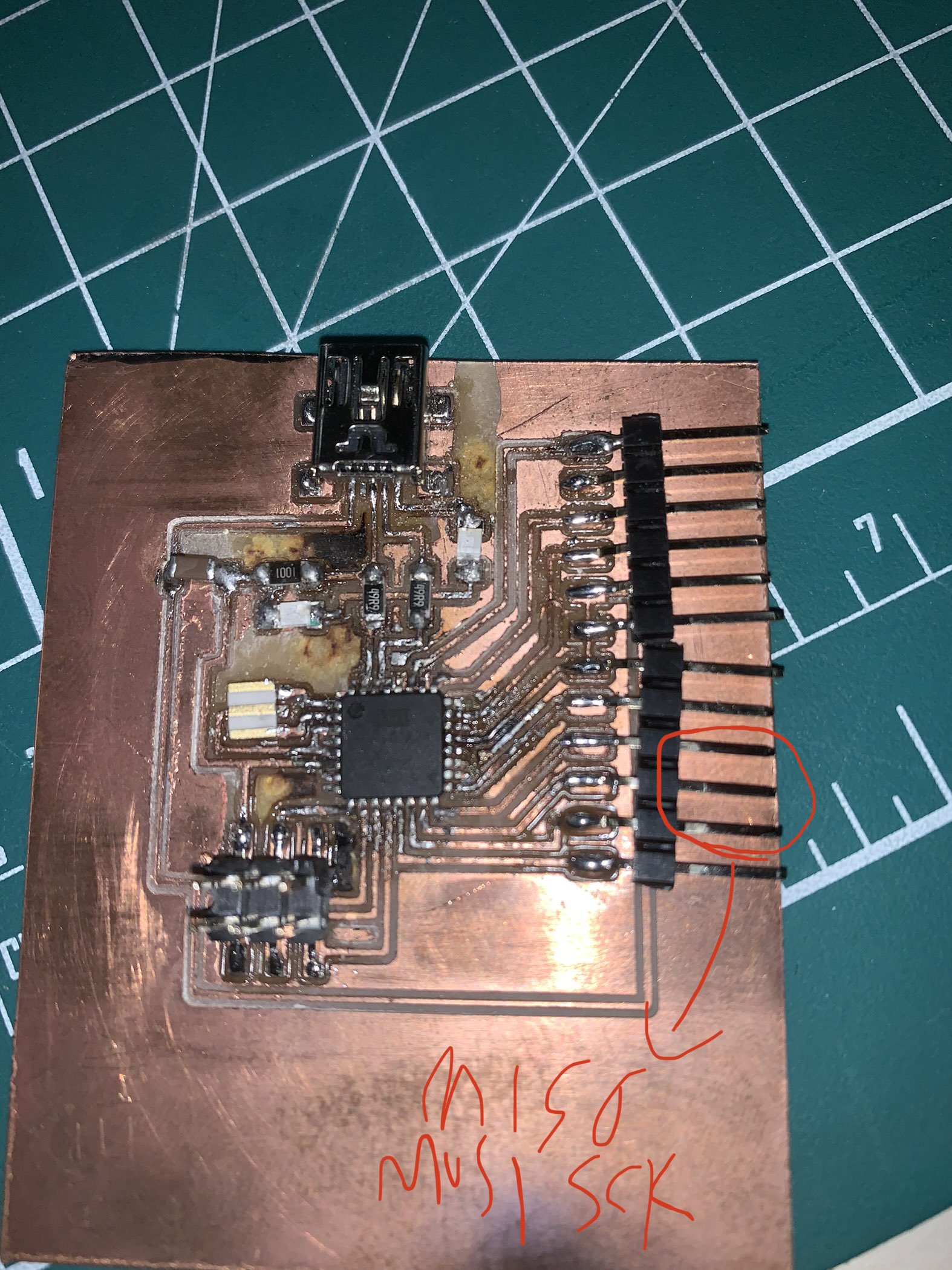
Second was forgetting about how to connect the PCB to a programmer board (my ISP programmer)
I also used the wrong type of diodes (LEDs instead of normal diodes) in my design. It may have fried my atmega328 at first, but I am inclined to believe that there were other bigger factors which contributed to its demise.
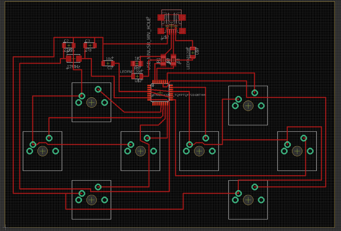
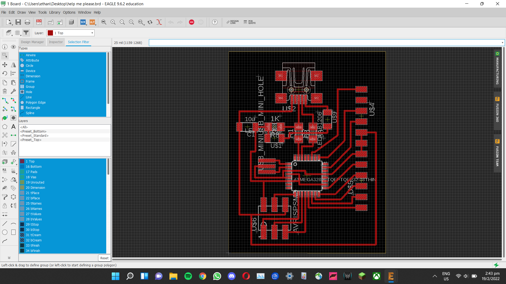
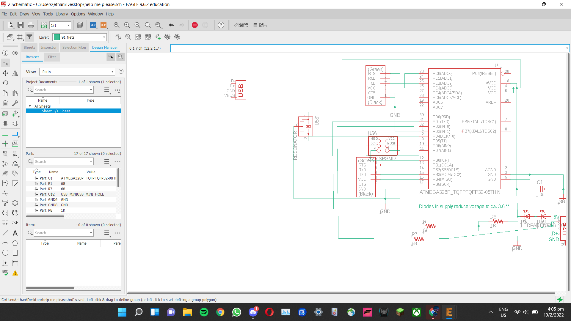
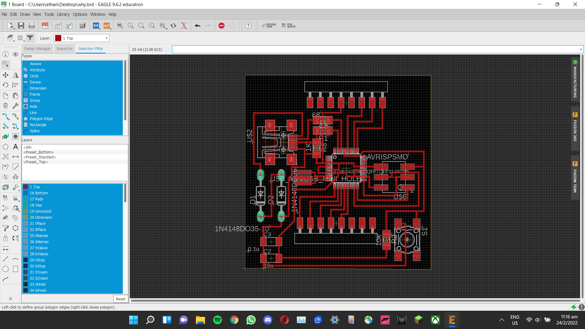
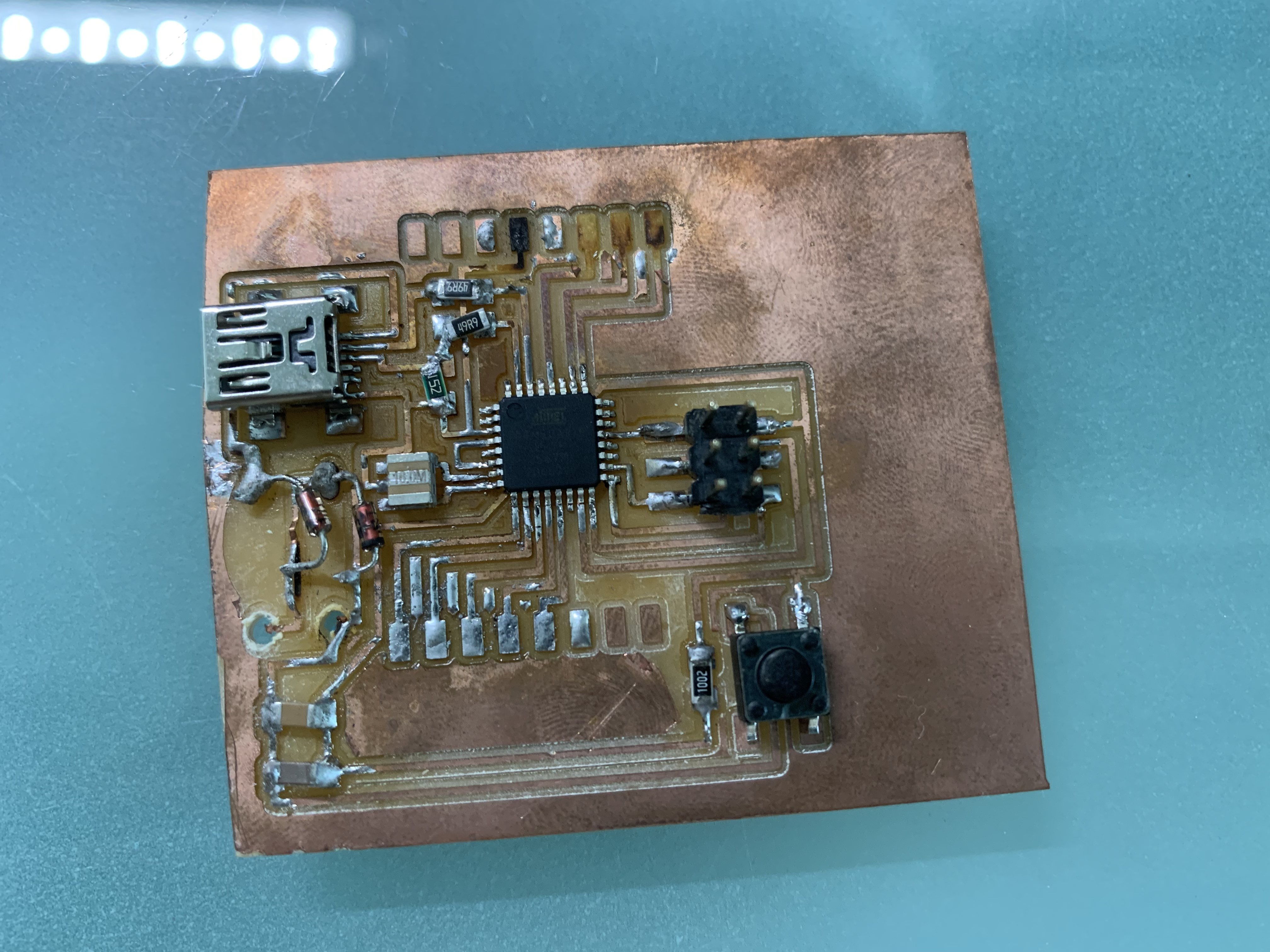
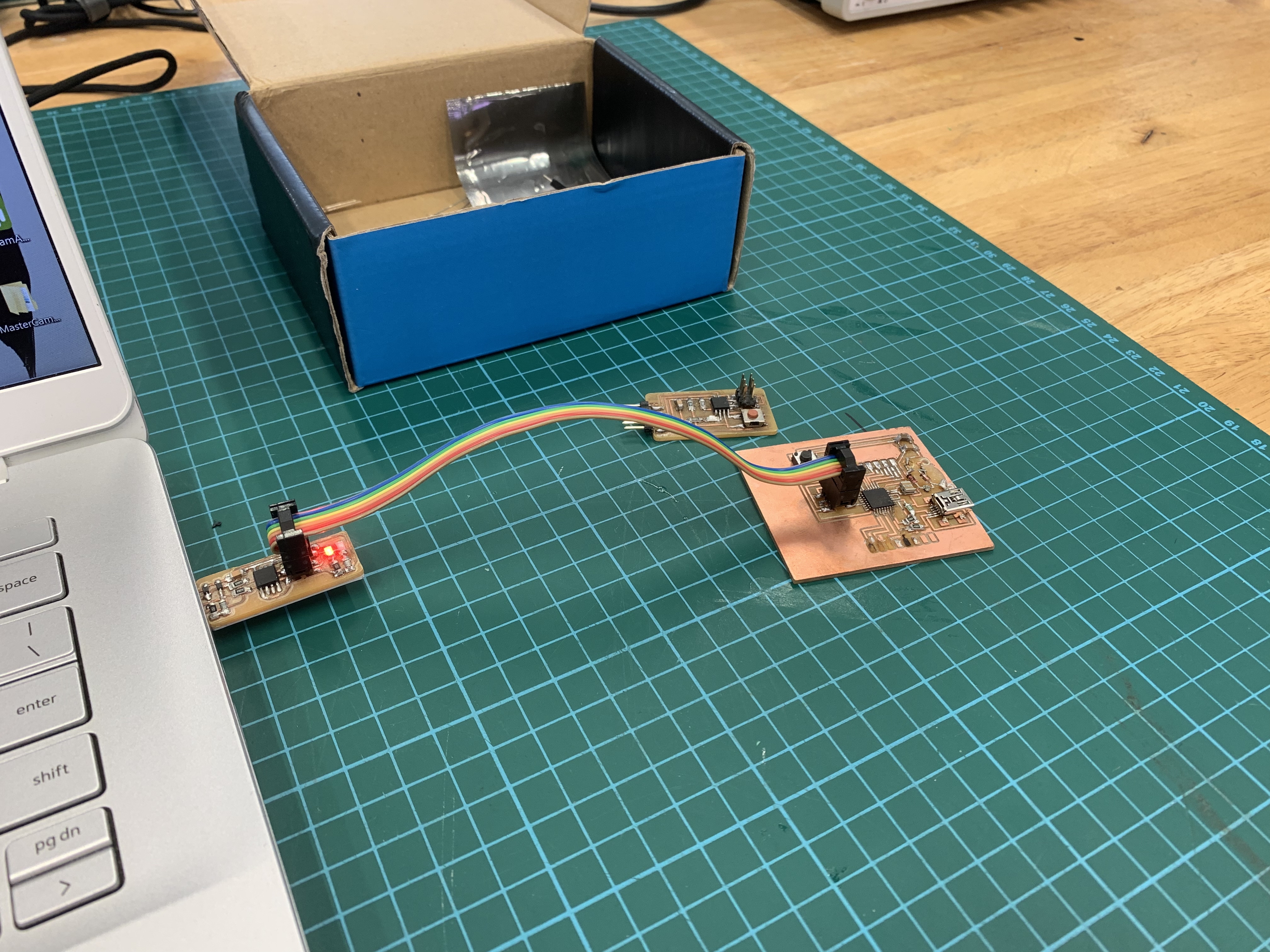
After my first "successful" board failed on me, I decided to rework the design. Here is what the final board design looks like.
Some changes were made, incluing changing the resistance across the USB pin (1.5k ohm resistor instead of 1k, changing the USB from usb-a to mini-usb, adding bypass capacitors...)
PCB Machining + Soldering
Machining
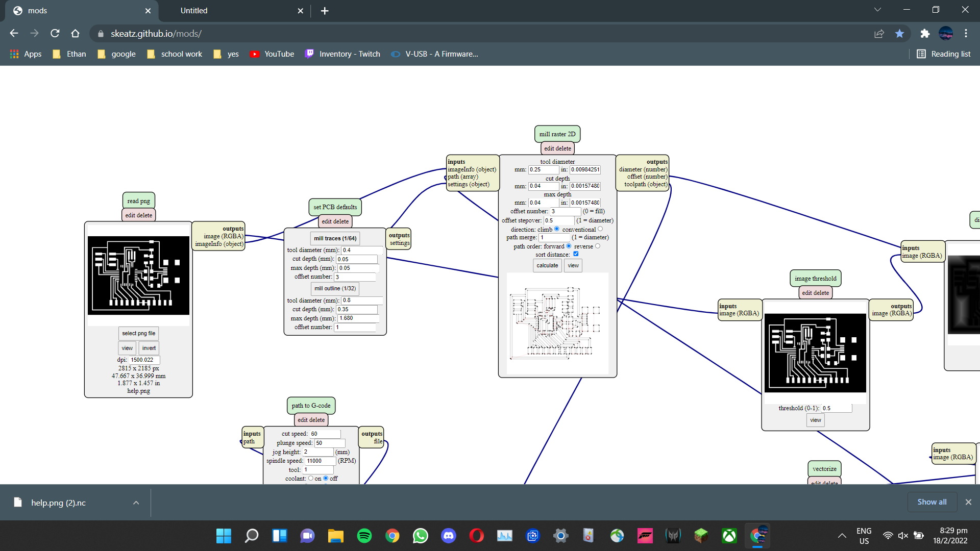
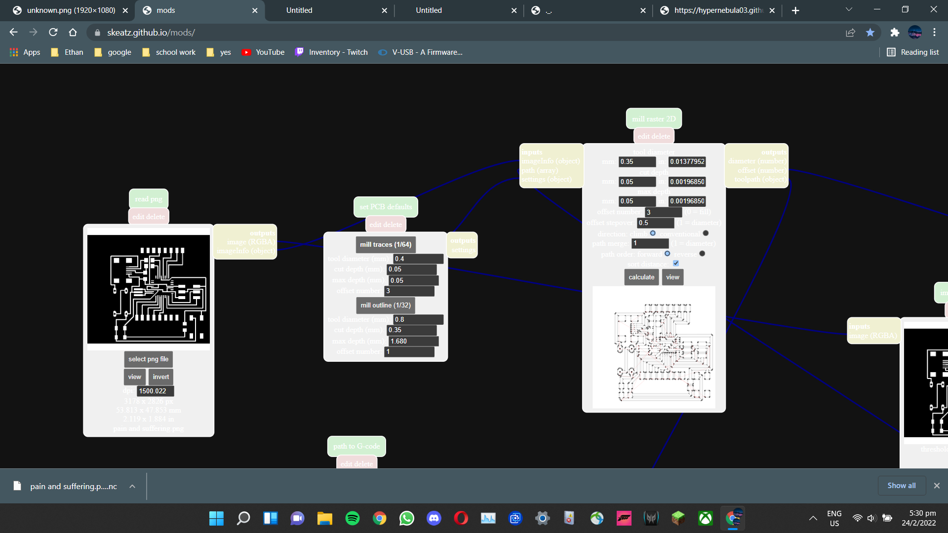
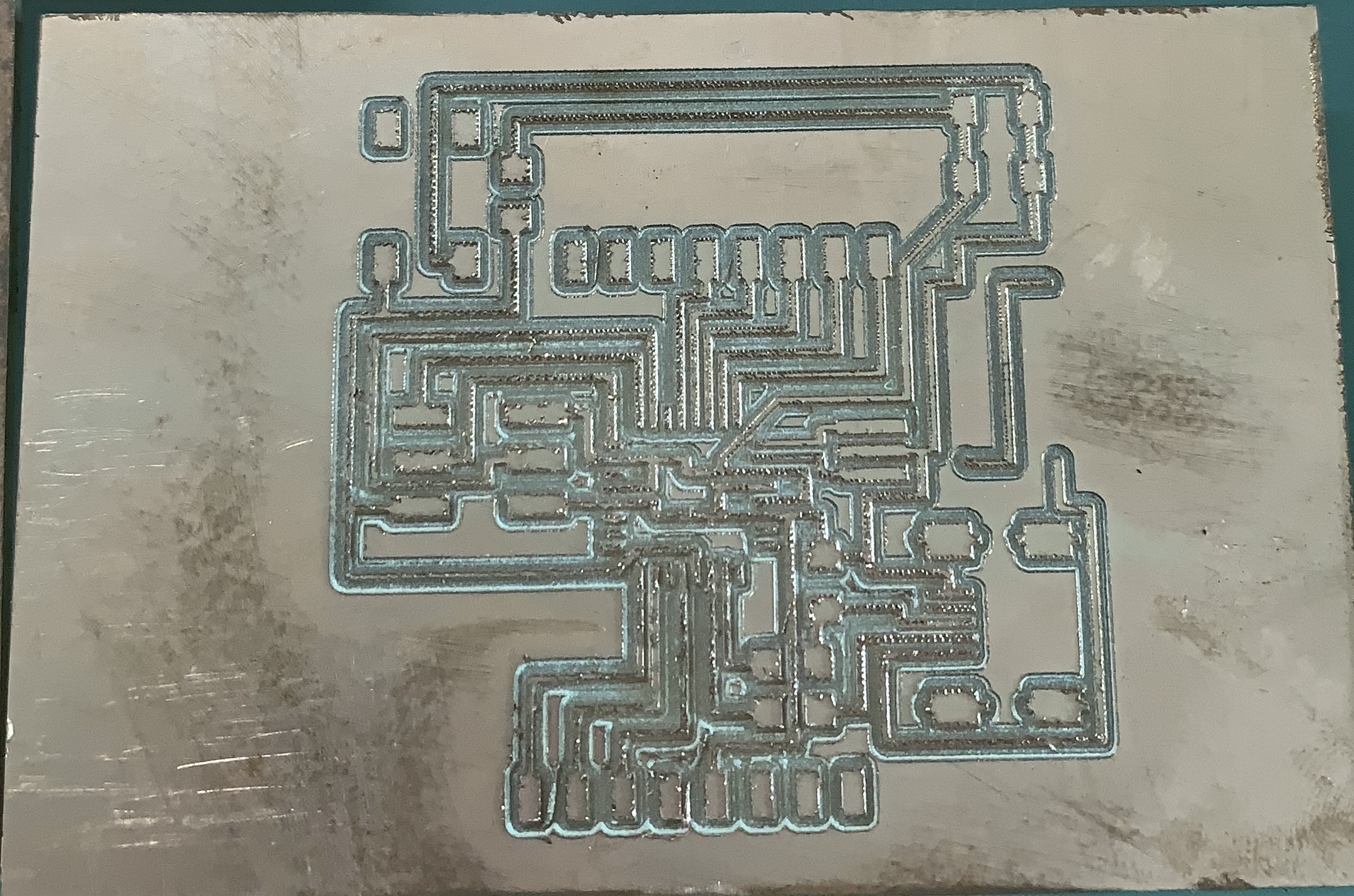
Using Mods, I generated the g-code for my PCB. All attempts had more or less the same settings (0.35mm tool diameter, 0.05mm cutting + total depth)
Attempt 1:
Attempt 2 (dark theme mods?):
However, the Stepcraft 420 machines were very chaotic, in the sense that it was very hard to get a consistently good board.
When I first started milling my PCB, I found out that the z-axis probe was not so accurate due to frequent use.
Thus, the traces were not cutting deep enough. Therefore, I had to adjust mid cycle by inputting higher z-values (by 0.02mm) and rewinding the g-code to an appropriate point.
In addition, the sacrificial board was worn out as double sided tape was used to anchor the copper board down. When ripped out, the board underneath would fray, making it uneven.
With an uneven board, this can cause some traces to be cut deeper and others more shallower. Sometimes parts of the PCB would not be milled in extreme cases.
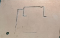
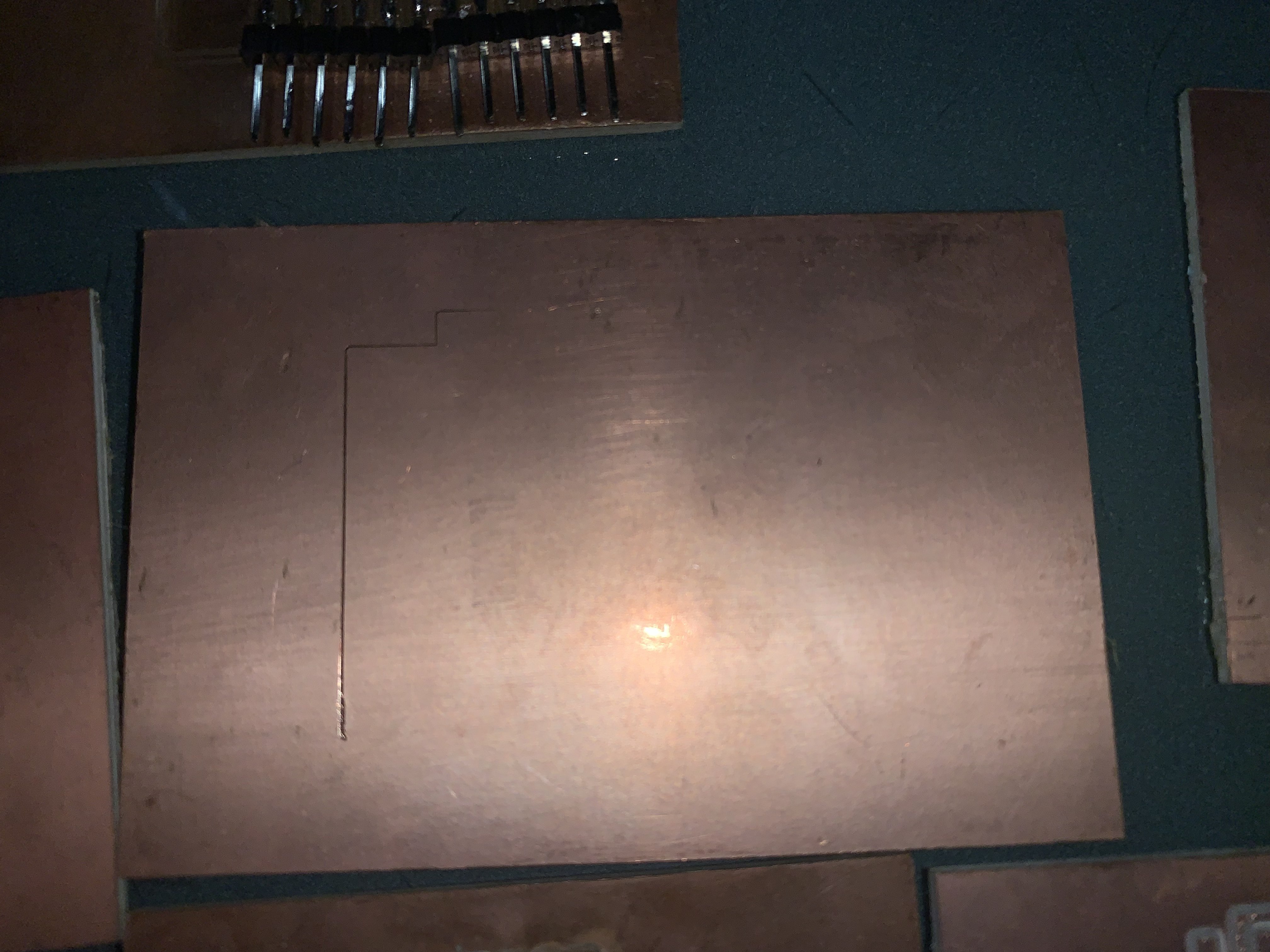
Below is what it looks when the trace is cut too deep.
Below is what it looks when the trace is cut too shallow.
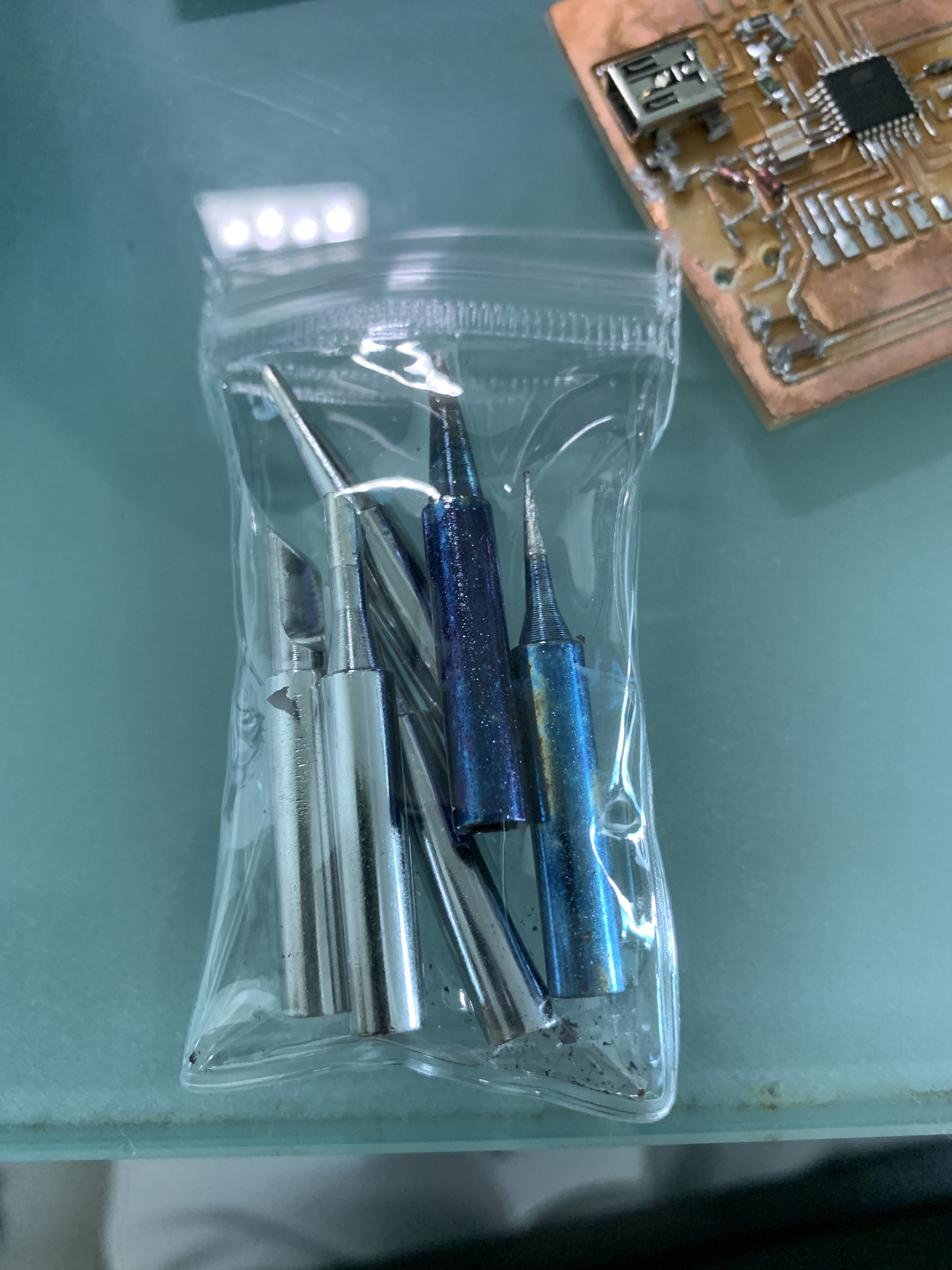
Furthermore, the type of endmill used can make or break our boards. Blunt bits would often make lots of burrs in our traces, thus after completion sanding was necessary.
The end mill tip can also break mid cut if it goes too deep too fast, which ruins the whole board.
It took me around 6 tries to get it right. Luckily, when it went right it went perfectly.
Unfortunately, I forgot that the mini USB header needs to be at the edge of the board so that the cable can connect. Thus I had to saw off the edges.
Even though this board isn't usable, I sawed it off as an example.

Soldering
These were the components I used:
- Atmega328/328p TQFP x1
- 1.5k ohm SMD resistor x1
- 49 ohm resistor x2
- 10k ohm resistor
- 10uF non-polar capacitor x1
- 0.1uF non-polar capacitor x1
- 2x3 ISP header x1
- 16MHz resonator x1
- 1N4148 diodes x2
- Mechanical Switches x8*
- 6mm pushbutton x1
- Keycaps x8
- Mini-USB cable x1
*I initially used second hand GAT Brown switches from a friend, however after soldering there was no electrical connection.
Hence, I switched to using Kalih Box Navies, given to me from my classmate Lynn.
Soldering the components was relatively ok, except for the atmega328 chip. Since the pins were so close together, the chances of shorting the pins was very high.
I tried to solder at home with a $20 soldering iron kit, however as the price would suggest, a cheap soldering iron is not exactly the best at its job.
The temperature control was abysmal and at its lowest temperature (200 degrees Celsius), the actual temperature felt hotter than the highest setting in the fablab.
It was evident when the copper board got charred that the temperature settings were very inaccurate. The tip of the soldering iron had oxidised and turned blue.
In my first attempt, I took 2 hours to solder the atmega328 chip, and thus fried it in the process.
I used the fablab soldering iron for my next few attempts, with better results. With assistance from Lynn and Mr Yeo GS, the soldering turned out well for the IC chip.
Once soldering was done, I used the multimeter to do a continuity check to see 2 things, whether points that were supposed to be connected were connected, and to check for shorts.
Soldering the rest of the components were much easier except for the resonator.
For the resonator, the connections were BELOW the component. Thus, unlike most other components, I had to use the heat gun to properly ensure the connections were there.
First, I had to cover the pads with solder, then place the resonator on top. While holding the resonator in place, I used the heat gun to melt the solder and let surface tension do the rest.
Finally, soldering was done. However, in my first attempt, I discovered a fatal error in my PCB design. I forgot to account for the programming section.
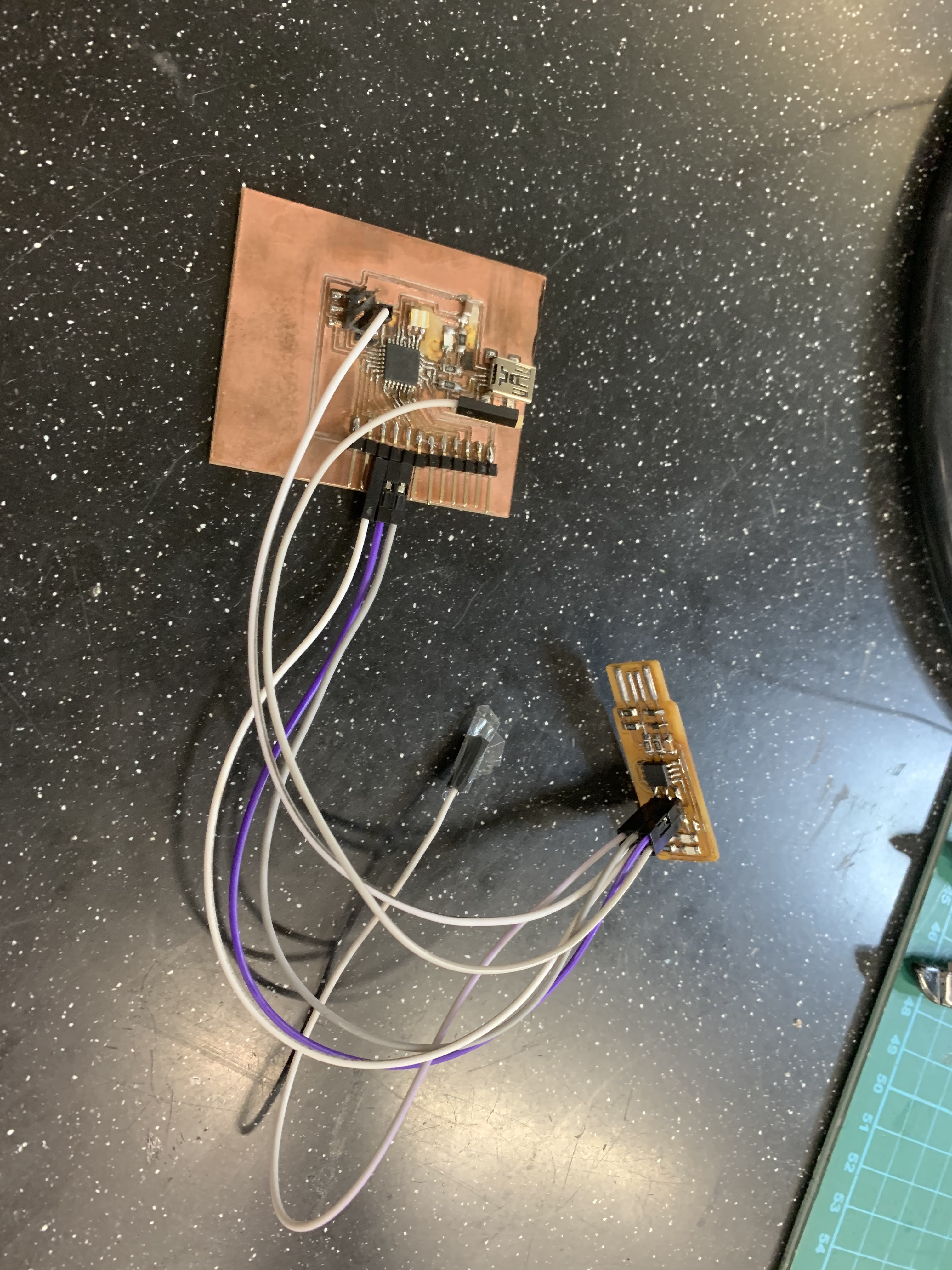
My PCB was designed without a way to connect it to my laptop for programming. Luckily the pins were still wirable with jumper cables, however the layout was very messy and confusing.
When testing it to see if my laptop could recognize my board, I discovered that the chip was likely to be fried. Judging by how messy it was, maybe it was a blessing in disguise.
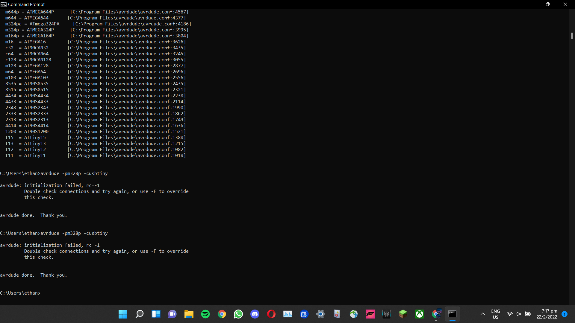
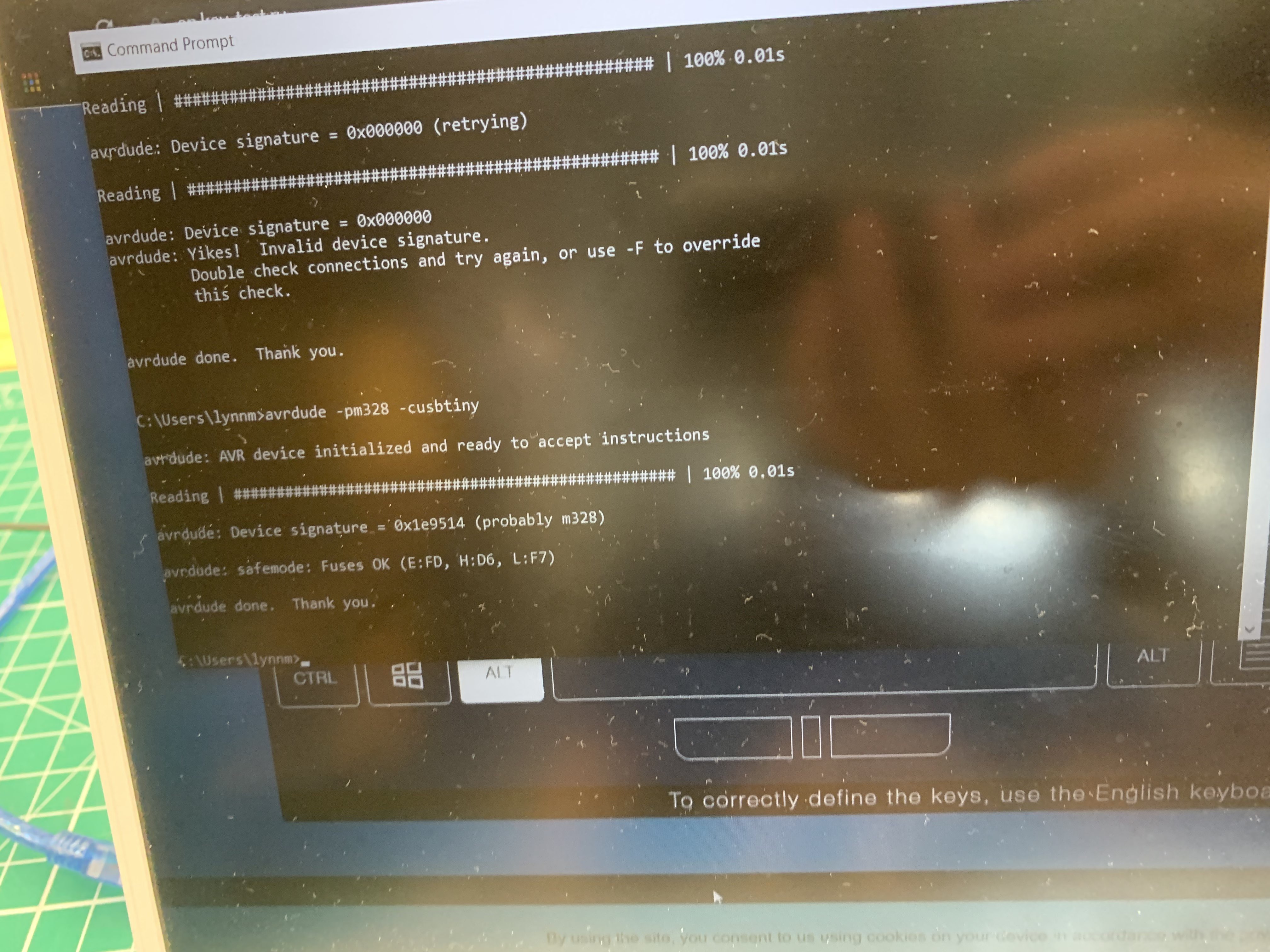
After a few days of redesigning, here was my best board. Keying in avrdude in control panel, the chip signature was recognized.
Programming
Due to hardware limitations, I utilized v-usb to resolve the lack of hardware usb support.
What v-usb does is it takes 2 data pins and converts them into usb ports for usb support.
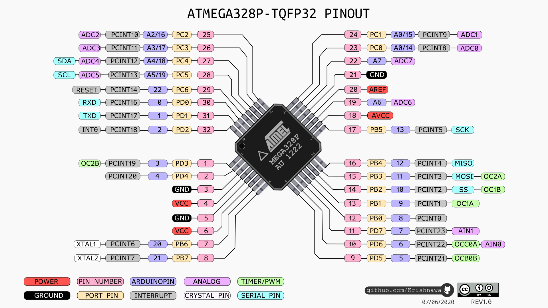
Since it is an 8-bit registry, the data pins have to be from arduino pins 0 to 8.
Using the atmega328 pinout sheet, these are the pins v-usb can use to facilitate the usb support.
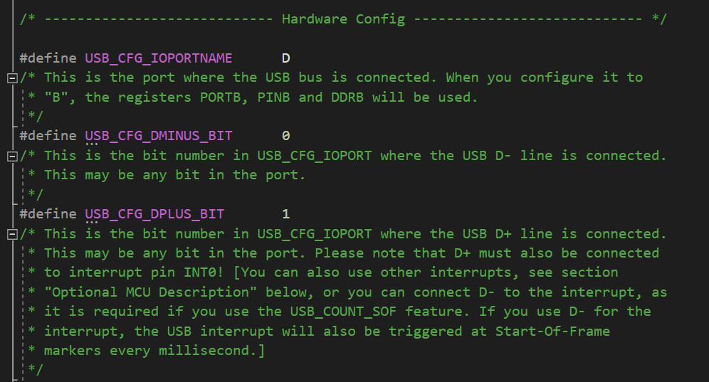
After installing the v-usb library, there are a few things we need to configure.
First is to determine which data pins will be used. Inside the v-usb file, there is a usbconfig.h file we need to edit.
Inside there are two lines which determine which data pins faciliate usb support.
Referring to our Eagle design and our atmega328 pinout sheet, I edited the file to suit my needs.
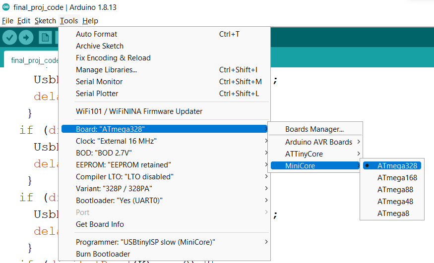
Next, we head to Arduino IDE. Since we are not using attiny IC chips, we need to install a new library which contains the correct IC chip used.
Online, the minicore library contains what we need, thus I installed it and now arduino IDE recognizes the correct IC chip family.
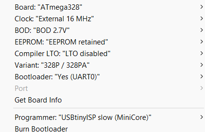
Afterwards, I had to change to the correct type of IC chip used (atmega328), as well as edited the type of bootloader (none) and changed the clock system to 16MHz external clock.
With that done, we can start programming.
I referenced a sample code and did some editing, mainly to remove unnecessary sections and looped the if statements for each key used.
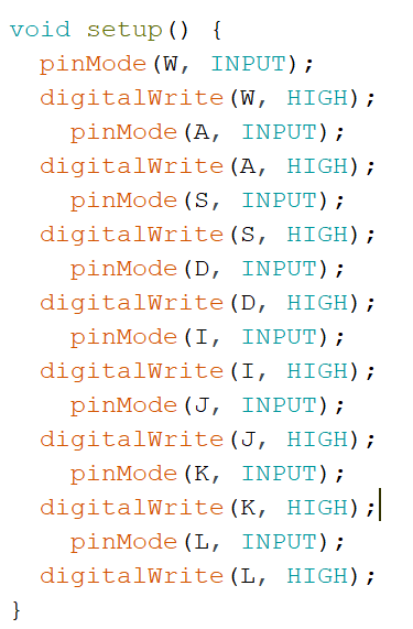
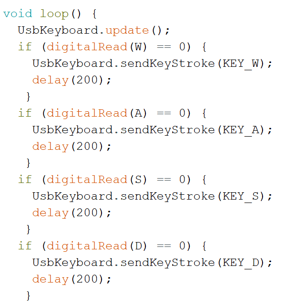
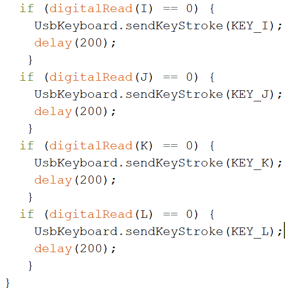
I also edited the defined pins to the ones I had included in my PCB design. Note that the defined pins are for Arduino pins, not the IC chip pins.
With that, I connected my ISP to the board and my laptop, burned my bootloader and uploaded the program.
To check if the program went through, I checked that my ISP programmer LEDs were blinking, and used the multimeter to check that voltage was flowing through the ISP headers.
CNC Machining
I decided to use the large format CNC machine to make my controller case.
I intially set up my case to pocket the inside so that the whole thing could be done in one piece, however I decided to switch to 2 pieces as pocket cutting would make the inner edges rough.
Sanding the inner corners would be tough, to say the least.
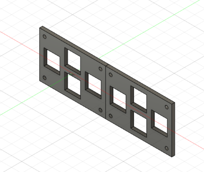
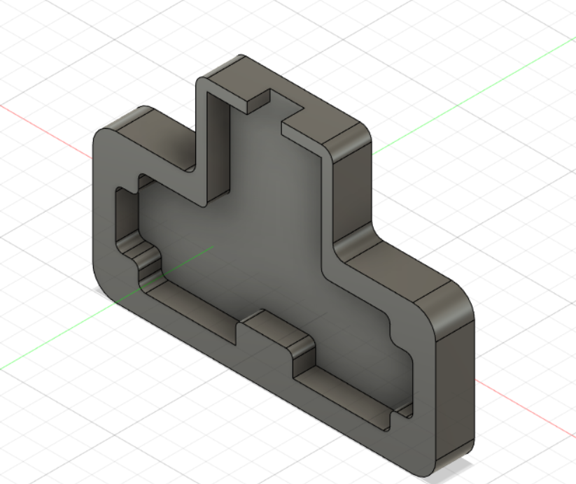
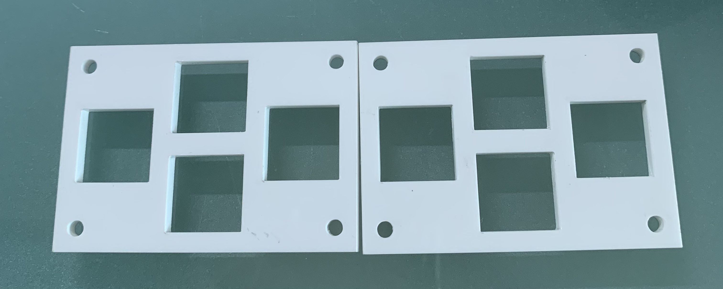
I first modelled how the switches would be seated. I modelled 2 cases to be put side by side. This will be laser cut.
Next, I modelled the exterior case.
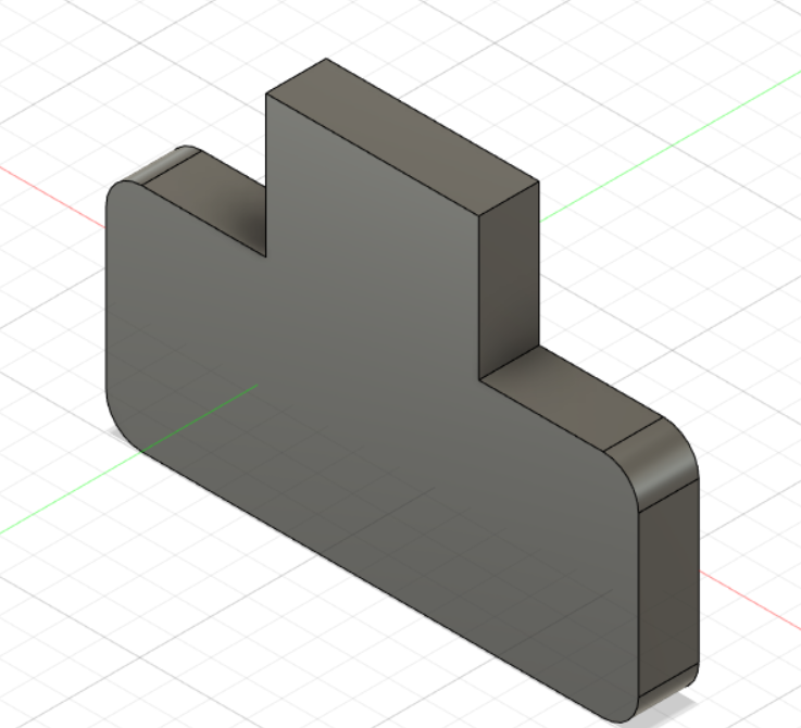
Afterwards, I modelled the interior section where the PCB will be housed.
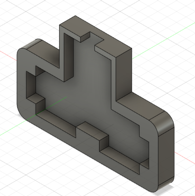
Finally, I filleted sharp edges around the inside and outside of the case.
Here is what the completed 3D model looks like.
Sadly, during the final days of the project, the only large format CNC machine broke down (z-axis calibration broke), thus I could not machine anything in that time.
On the bright side, at least the laser cut switch plates came out fine.
Integration
Sadly, while intergrating everything together, I discovered that my laptop kept rejecting the USB device (my PCB). I tried many methods to solve it, including:
Changing USB ports
Switching laptops
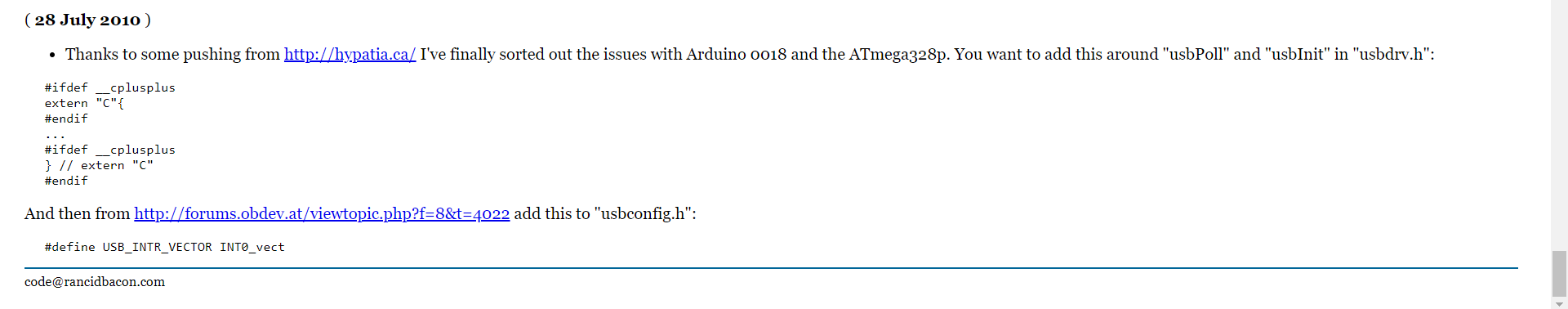
Editing the source code (usbdrv.h)
Changing the IC chip from atmega328p to atmega328
Unfortunately, none of the above measures worked and I could not solve it before the project due date.
What Works:
The atmega328 chip signature was recognized by my laptop and the PCB could receive code from my laptop. The laser cut case also held the switches well, and in theory the CNC machined case can hold everything together.
What Doesn't Work:
Laptop keeps rejecting the PCB, thus I could not test my code to show it works.
Google Drive link for my slide + videos
Reflections
Although the project was not finished in time, I still learnt a lot.
- soldering smd components is quite difficult, especially without proper thermal control. the atmega328p pins were very close together which made life very hard for me
- resonator was hard to solder (connections are below the component)
- it is good to read up on specifications of your microchip before you design your board (e.g finding vusb library, reading atmega328p specs to find that both vcc and ground pins need to be connected to stabilize the chip)
- knowing how to design properly + find resources to help you is very important. That way, you avoid doing this:

- for some attempts, be prepared to fail because limitations make pcb milling volatile (z axis probe sometimes doesn’t work, need adjust level midway, endmill not sharp causing burrs or even no cut)
- when probe not working, have to manually set z axis yourself using paper and slowly lowering the machine (in steps)
If you would like to see what a working product looks like, you can look at
Lynn's final project. He did something similar to mine, only difference being the number of switches, case and PCB design. Most importantly, his project works.
Special Thanks To:
I have many people to thank for assisting me throughout this project. Without them, it's safe to say I would not have gotten this far.
First is Zi Hon, who told me to read the datasheet of the atmega328p chip. He pointed out that both VCC and GND pins have to be connected, as well as advised me to connect the external resonator close to the chip, each pin equidistant from the chip and have a low impedance connection to GND.
Next is Mr Steven Chew for advising me to look into v-usb to address the lack of hardware usb support most IC chips in the Fablab had. He also gave us info about how to properly utilize v-usb in terms of electronics.
Finally, Lynn Myat "Makerspace Moe" Aung. He gave me advice on the hardware section of this project, teaching me how to handle the soldering of the atmega328 chips.