In Electronics Design, this is where I learnt how to make custom PCBs for my own use.
Using Autodesk Eagle, a Computer Aided Engineering software (CAE), custom PCBs can be designed from scratch.
There are other softwares available (e.g. Kicad), however for this module I chose to use Eagle.
For Autodesk Eagle, to make a PCB, there are two sections to it. First is the schematic. This is where you design/add the electronics.
It is also where you verify the electrical connections to see if the PCB electrically works as intended.
Next is the Board Design. Like the name says, it is where you design your PCB and wire your connections. This will influence your g-code and can be very time consuming.
For my assignment, I had to make an Echo Board from scratch.
This means I have to design my own board, mill it out, solder the electronics and finally code it.
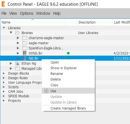
To start off, I have to install the Fablab Library first. Eagle's default library does not have the electronic components I needed.
Under Eagle's control panel, I added the new directory where I unzipped my Fablab library. Afterwards, click "Use All" to read the library.
After creating a new schematic, it's time to add all our components.
The components we need are:
- ATtiny85 X1
- 10KΩ resistors X2
- 1KΩ resistors X1
- red LED X1
- 100nF non-polar capacitor X1
- 2X3 pin header X1
- 1X6 pin header X1
With that done, it is time to wire everything up.
Here is the finished electrical layout. To verify everything works, we do a ERC (Electrical Rule Check).
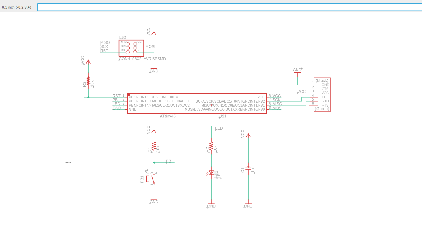
We can ignore some of the warnings as some pins will not be used.
Now, we switch over to the board layout through the "Switch to Board" tab.
Before we arrange our board layout, we have to resize the board.
Afterwards, I set the wire bending style and width of each wire to 16.
There are a few ways to wire your PCB. The main thing to note is that connections cannot intersect one another.
To make life simpler, I decided to use Autoroute and edit (using Ripup command) from there. While not perfect, it gives me a starting point and is better than nothing.
After many hours of rewiring, this is what I got:
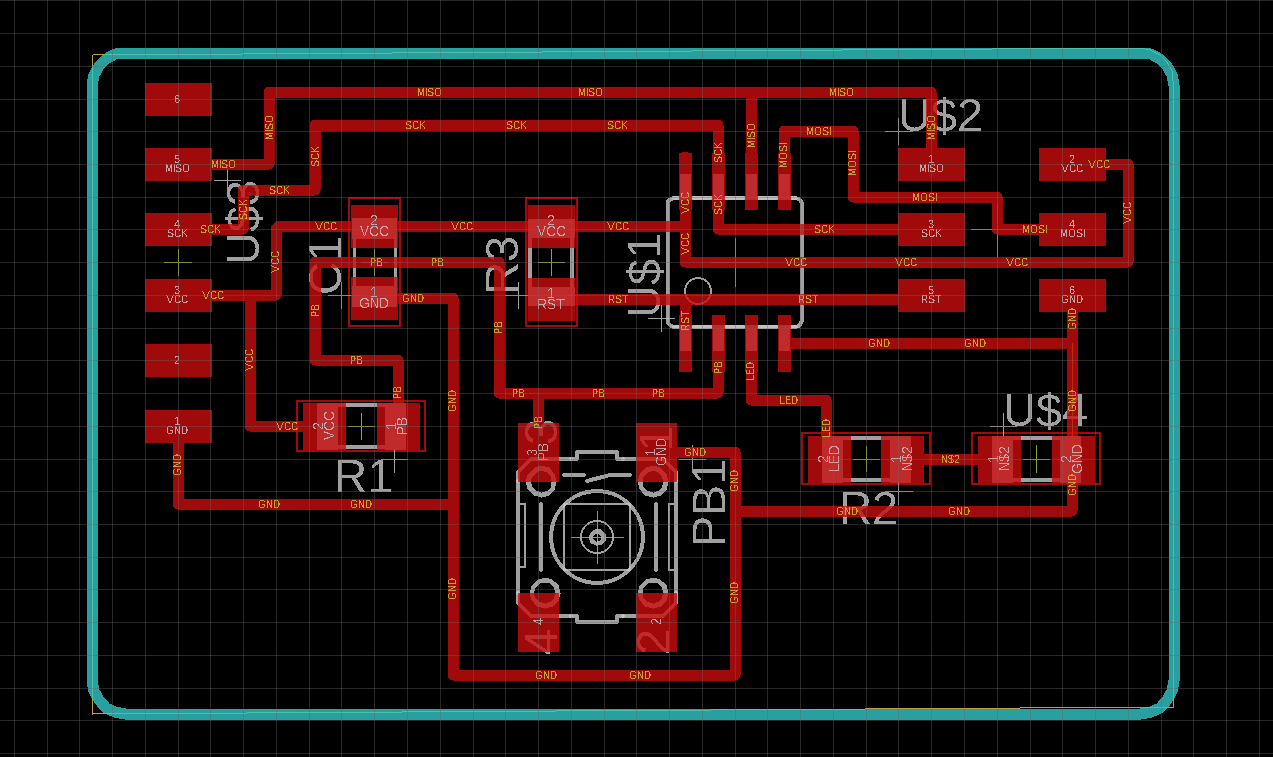
We need to create an external layer for our outline. Using Layer 46 (Milling), I drew a basic outline surrounding my board (see above outline in blue).
Before we can export our board, we have to verify it again, using DRC (Design Rule Check).
This is to ensure the traces are wide enough and the PCB is machinable.

Now, we convert our board layout into g-code. To do this, I filtered by layer (one for trace, one for outline) and exported a PNG image of it.
Recommended DPI is 1500 and monochrome must be ticked if you plan to use Mods to generate the g-code.

Using Mods, I replicated the settings I used to create my ISP for both traces and outline.
With that done, it's time to machine the PCB out.
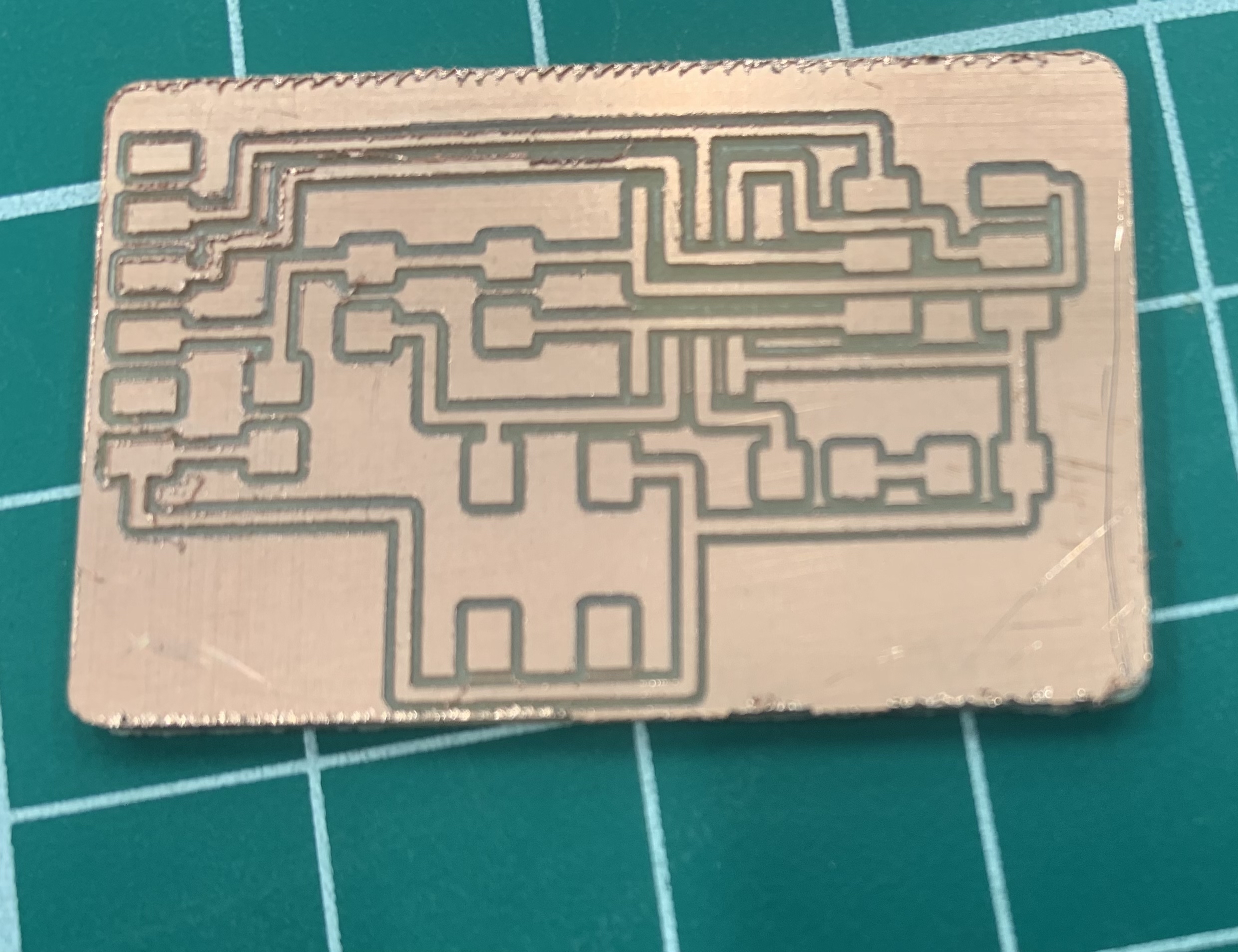
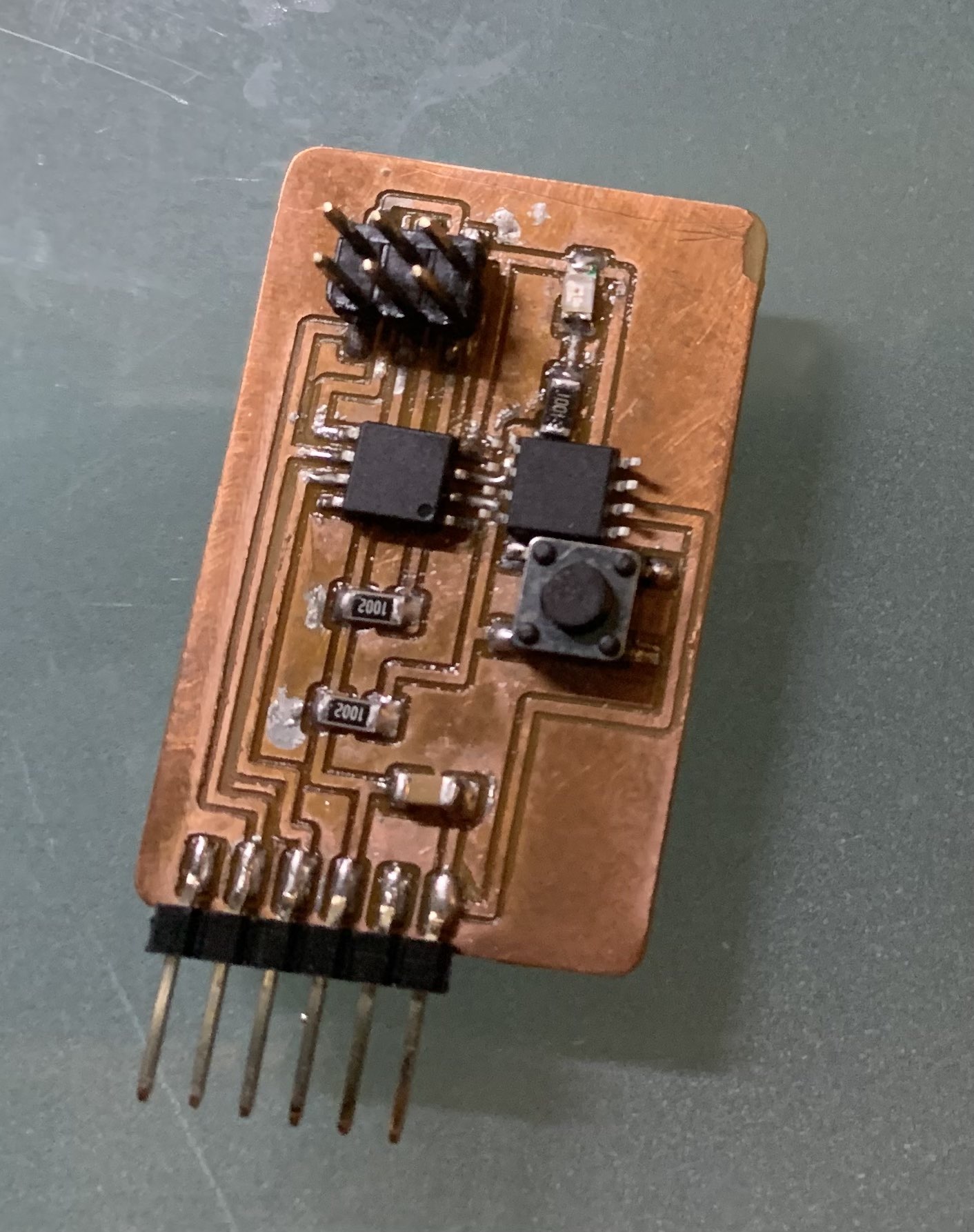
Here is the PCB cut out. I tried to remove the dead copper but couldn't remove it.
Time to stuff the board. This was much harder since unlike the ISP, there is less space for solder due to the design of the PCB.
Initially, my soldering was not the best. Some parts were too small to solder and excess solder shorted some pins.
With some assistance from Mr Steven Chew, the board was finally soldered properly without any shorts.
Time to program the board. Using the ISP I made, I linked the Hello Board to my laptop.
Since the programs were installed, all I needed was to type 'avrdude' to ensure the board was recongnized.
(image)